What you will need
Oscilloscope
Any DSO will do. Using analog oscilloscope is not recomended due to the nature of signals generated on the board.
Multimeter or voltmeter
For measuring DC power rails.
Common problems
Device is not detected by computer
Faulty USB cable. Try to replace USB cable for other one.
Badly soldered USB connector. Resolder it.
PIC is not powered up. Check 3.3V rail (refer to Power rails section). Green LED should be lit.
Firmware is not present on PIC. Flash firmware to the microcontroller (refer to How to program section).
Device is not detected by CGMiner
Klondike support not enabled. Recompile with --enable-klondike option. Refer to How to run section.
Device not sending results at all
Delay between data and clock signal too short. Did you replaced capacitor in RC delay circuit?
ASICs are not powered up. Check all 1.2V power rails.
Lower than nominal hash rate
Some ASICs are not powered up, are missing clock signal, not getting configuration data or are held in reset. Refer to Clock source, Result bus and Configuration bus troubleshoot.
Big troubleshoot
In this troubleshoot we will try to determine the cause of a faulty board (board that is not sending out found nonces, board that do not perform well, that is not discovered by computer etc). We will go through a couple of things - power rails and regulators, reporting logic and configuration logic.
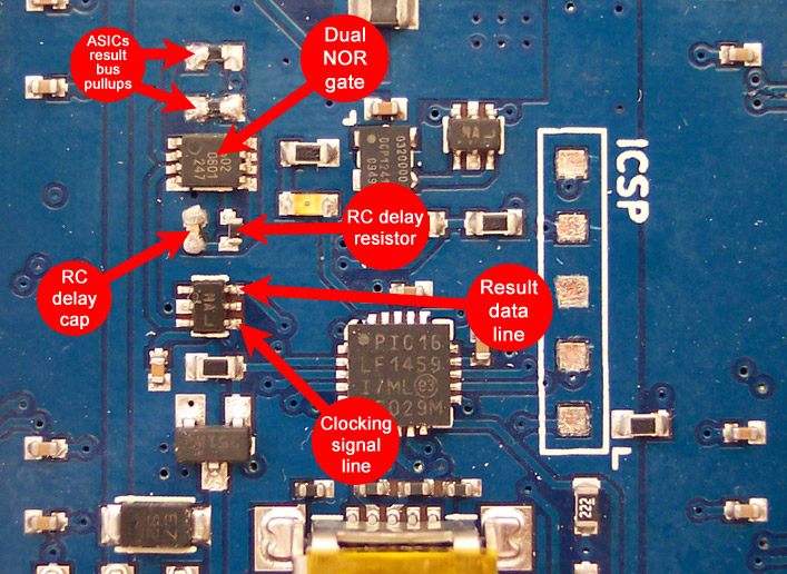
All pictures here were taken with K16q board (with PIC in QFN package), but positions of all other components are exactly the same as with K16s.
Common issues
Hashrate issues
You can calculate nominal hashrate of the board with simple equation: clock*chipcount = MH/s. If you're clocking chips at 350MHz, hashrate of a whole board should be 350*16 = 5600MH/s (5.6GH/s). When hashrate of the running board is lower than nominal, couple options you have:
- Hashrate is exactly one half of nominal one
- Hashrate is not exactly half of the nominal one
- Board is not hashing at all
Hashrate is exactly one half of nominal one
In this case one bank of 8 chips is not hashing at all. This is usually caused by overheated or overloaded 1.2V Core power rail. Refer to Power rails troubleshoot on this page.
Hashrate is not exactly half of the nominal one
In this case, some of the chips in one of the banks are not hashing at all. You can determine those chips by couple of methods. First one is to use CGMiner API stats to display found nonces and errors per chip. Since chips are quite dumb devices using shared result bus, the way those stats are composed by CGMiner is by determining the range to which the golden nonce returned by each of the chip belongs. Since each chip is working only on a small portion of a whole range, this way you can tell which chip is returning nonces and which isn't.
But even this method can result in inaccurate chip stats. In a case, in which one or multiple chips are not removing its portion of a configuration data and are not sending out found golden nonces, those stats are shifted by those chips.
So in a chain, you have 8 chips. First four chips are working ok, the fifth one is not working and not removing its portion of a config data, but is passing config data along to the last three chips, and the last three chips are working ok. In this case, the API stats will return, that first seven chips are working ok, and the last one is an issue. So even in cases like this, you have to combine this troubleshoot method with other methods described lower.
To access API stats (on localhost), you have to edit cgminer.conf file and add this options to it:"api-listen" : true,
"api-port" : "4028"
Then simply log on via SSH to OS console (we'e talking Linux here) and use following command (you have to have netcat installed):echo -n "{ \"command\":\"stats\" }" | nc 127.0.0.1 4028 | grep ' Chip'
It should return long string containing all the stats for CGminer. The two you are looking for are "Nonces / Chip 0" and "Errors / Chip 0" (they should be colored by grep). It's an array containing returned nonces by each of the chips and errors per chip. The order when using both banks (16 chips total) is (B Bank, C chip):Nonces / Chip 0 => B0/C8 B0/C7 B0/C6 B0/C5 B0/C4 B0/C3 B0/C2 B0/C1 B1/C8 B1/C7 B1/C6 B1/C5 B1/C3 B1/C3 B1/C2 B1/C1
And returned data should look like this:
"Nonces / Chip 0":"0003577 0003520 0003625 0003552 0003589 0003516 0003632 0003648 0003654 0003597 0003502 0003660 0003468 0003575 0003580 0003603"
"Errors / Chip 0":"0000000 0000002 0000000 0000002 0000000 0000000 0000001 0000001 0000000 0000000 0000000 0000000 0000000 0000000 0000001 0000000"
Basically, you're looking for a chips, that have produced much more errors than other ones, or for a chips, that have found less golden nonces than the other. But bear in mind, that there will be slight variation between all of the chips, especially in a short runs.
If you're running on Windows, but you do have a Linux machine with netcat, you can add this option to the cgminer.conf file after api-port option:"api-network" : true
By doing that, the API will be accesible over network, so you can use address of your Windows machine in nc command (nc 192.168.0.10 for example). Don't forget to create a firewall rule for port you will be using.
If you have Java installed, you can use following command in CGMiner folder to get only Nonces and Errors per chip:java API stats | grep ' Chip' | grep -v STA
Another method to determine a chip, that is not hashing, is its temperature. It should be considerably lower than the rest of the chips. You can feel the difference using your finger and touching the top of the chips. But even this metod has its limitations. The chip will be colder only in cases, when it is missing power, or clock signal. In a cases, where the result bus or config bus connection is an issue, this method wont work, because chip will be as hot as any other working chip.
When chips are clocked to 350MHz, chip temperature is around 50°C. Chips missing power or clock signal are colder, basically heated up only by surrounding radiation.
Board is not hashing at all
In this case, you have to inspect all possible causes - power rails, result and configuration busses. Refer to those sections lower in this document.
Troubleshooting K16
Power rails
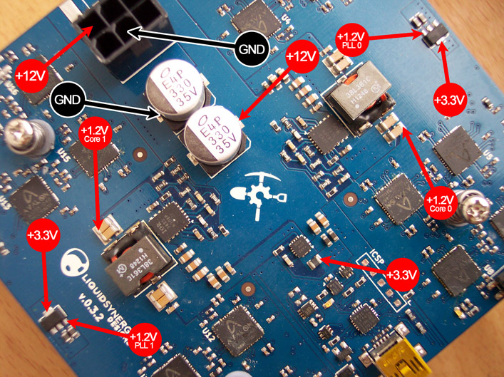
K16 uses five different power rails. For a board to function correctly, all five rails has to be operational. So first thing to check is to check the power rails.
| 3.3V rail | 1.2V Core rail 0 | 1.2V PLL rail 0 | 1.2V Core rail 1 | 1.2V PLL rail 1 |
| Rail used to supply PIC and chips reporting logic | Rail used to supply core voltage for ASICs at Bank 0 | Rail used to supply PLL for ASICs at Bank 0 | Rail used to supply core voltage for ASICs at Bank 1 | Rail used to supply PLL for ASICs at Bank 1 |
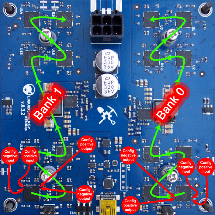
Board is divided into two Banks, each consisting of 8 ASICs. Each Bank (group of 8 ASICs) has it's own Core and PLL power supply rails, but both banks share one 3.3V power rail.
Bank 0 is above USB connector when connector is pointing to the right side (as on the photograph). Bank 1 is under the USB.
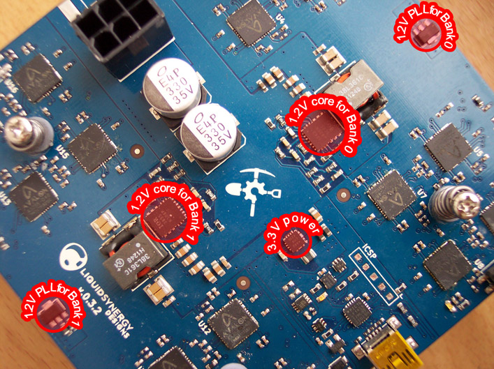
On the next image you can see all the testpoints for power rails. Black lead from multimeter (GND) comes to any GND terminal. Ground (GND) is shared, so it doesn't matter which GND will you use. Red lead comes to one of the red power test points. Check each one and compare measured values with the table below.
| Name | +12V | +3.3V | +1.2V PLL 0 | +1.2V Core 0 | +1.2V PLL 1 | +1.2V Core 1 |
| Typical voltage (range) [V] | 12 (10 to 14) | 3.25 (3.2 to 3.4) | 1.18 (1.16 to 1.22) | 1.20 (1.16 to 1.22) | 1.18 (1.16 to 1.22) | 1.20 (1.16 to 1.22) |
If any measured rail measures 0V, two possible things happened:
- Power regulator for this rail overheated or overloaded (or both)
- Short is present on that particular rail
Overheat can be caused by insufficient cooling (or operating device in too warm enviroments). When any of the power regulators overheat, they shuts off. To start them again, you have to disconnect power for a while and let them cool down.
Overload can be caused by clocking ASICs too high. The higher the clock, the higher the current required by the ASICs, and the higher the regulator temperature. So clocking ASICs too high can cause regulator over-current protection or over-heat protection to kick in. To restore this state, disconnect power for a while. When ASICs were overclocked, lower the clock slightly.
If short is present, it can be under any of the ASICs or other components using that particular power rail. Best way to determine a short is to measure continuity between GND and that particular rail. If resistance is too low (couple of ohms), short is present. Determining the exact component, which is causing this is hard (or harder). The only way to do this is to use visual inspection or trial and error method.
When, for example, only 1.2V Core power for Bank 0 is missing, you have to inspect only ASICs at Bank 0.
When 3.3V power is missing, you have to inspect all the ASICs in both banks, the PIC, oscillator, NOR gate and Inverters, because all these components share 3.3V power rail.
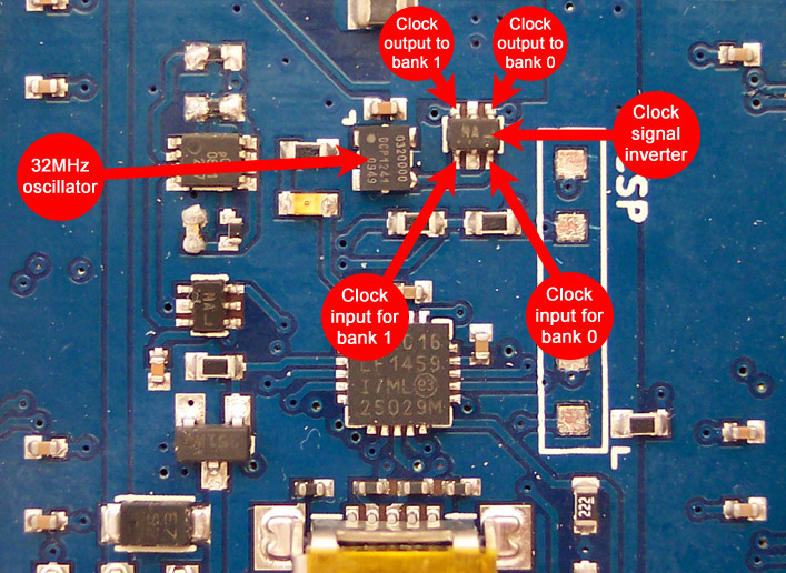
Clock source
PIC microcontroller is using internal 16MHz oscillator with 3 times PLL generating 48MHz. Since this is internally generated signal, no need to check that one. ASICs, however, are using external 32MHz oscillator. There are couple of points to check for this signal, as you can see on the picture below. However be aware, that oscillator enable pin is held low by default by PIC. It is turned high when first work item arrives.
Signal from oscillator is fed to dual gate inverter. Each output from the inverter is used to drive ASICs in different banks.
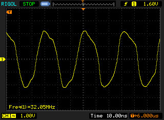
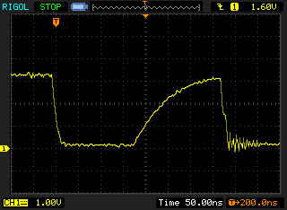
Clock signal right after the Inverter should look like this on both outputs:
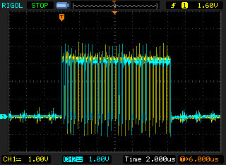
Result bus
Result bus is shared among all 16 ASICs. It's used by ASICs for reporting nonces back to the PIC. It's sort of differential signaling bus, thus using two wires. This bus defines two states - around 3.3V when idle, and near 0V.
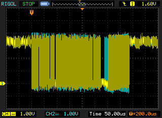
When nonce is found by one of the ASICs, that particular ASIC pulls result bus to the ground based on data trasmitted. If this line is not held at around 3.3V when ASICs are idle (not trasmitting results), solder bridge between some of the pads under ASICs is probable. In this case, results cannot be sucessfully trasmitted to the PIC. You can see one of the lines of the result bus pulled low at next picture (other one looks simillar, measured at place in Picture 5 above named "ASICs result bus pullups"):
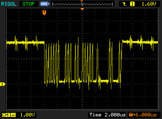
These pictures were taken with 1K pull-up ressistors (R45 and R46 in BOM and scheme). With 390R, the rise time will be shorter (rise will be steeper). It is recomended to use 390R pull-ups, but board is working fine even with 1K ones.
Result bus after NOR gate and Inverter
To make signal more clear for the PIC and to extract clocking signal, prior feeding it into the PIC, it goes through a couple of components. First one is NOR gate with RC delay. Here clocking signal is extracted by combining both result lines and delayed by using an RC delay. After this is done, now separated clocking and data signal is fed to the Schmidt-trigger buffer Inverter to invert it and make it more steep and clear of noise. This modified signal is finally fed to the PIC for converting to digital ones and zeros.
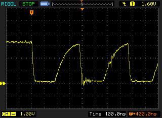
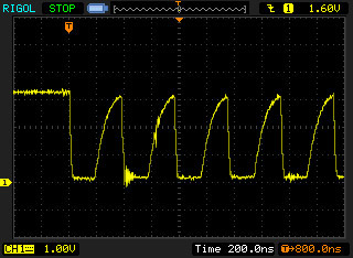
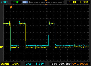
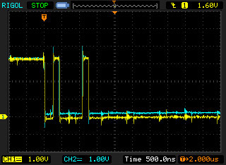
You can see both result lines after Inverter at the next couple of pictures:
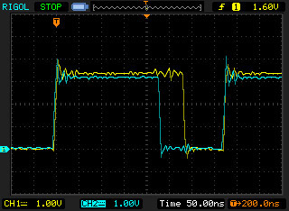
Channel 2 (blue) is result data after Inverter at the input to the PIC. When ASICs are not transmitting results, held at logical low (near 0V). When result is beign trasmitted, this line is pulled to logical high to around 3.3V based on a data transmitted.
Channel 1 (yellow) is clocking signal. Data from channel 2 are captured on falling edge of this clocking signal. Held low when idle. Active only when result is beign transmitted from the ASICs. This signal is periodically repeated. It is also delayed to about 50ns behind data signal when 470pF capacitor in RC circuit is used. It is possible to use also capacitor with lower capacitance, for example 220pF (the delay would be around 25ns in this case), but using 470pF is recomended. When delay between clock signal and data signal is too small, bad nonces are returned by the PIC (usually 0xFFFFFFF3 or something simillar).
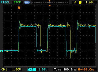
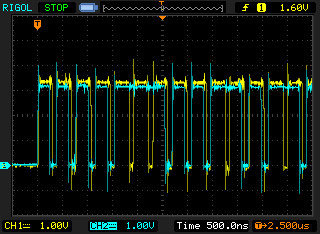
Configuration bus
Each bank uses it's own configuration bus. It's two lines bus simillar to the Result bus. Configuration data are beign sent by PIC to the ASICs. Since ASICs are chained (marked by green line in Picture number 15), first ASIC in a bank receives configuration data from PIC via configuration input bus and then sends it out to the next ASIC via configuration output bus. Configuration contains various information for the ASICs like clock settings or work data. Configuration bus should be held high (at around 3.3V) when idle. When data are beign transmitted, it's pulled low based on data transmitted.
In the next picture you can see one of the config input lines to the ASIC (yellow) and corresponding config output line from the ASIC (blue):
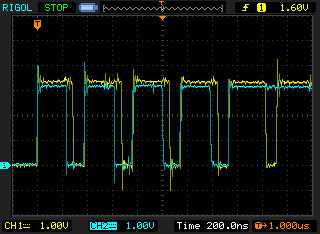
When ASIC is working correctly, it receives configuration data via the configuration input bus, it then removes it's portion of a work data, and sends rest of the configuration to the next ASIC in a chain via configuration output bus. You can see nonce removed at the config bus output in the next pictures:
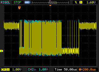
First picture (on the left side) is config negative input (blue, CONFIG_NI in A3256Q48 datasheet, second chip in a chain) and config negative output (yellow, CONFIG_NO in A3256Q48 datasheet) after one nonce range is removed by ASIC. On the second picture is the same thing, except that for config positive input/output (CONFIG_PI, CONFIG_PO).
When chip specific nonce portion of the data is not removed (from both config lines), this could mean, that ASIC doesn’t have clock input properly connected, power at one of the rails is not present, or chip is held in reset. This can be caused by solder bridges or by cold joints.